
Figure 1: N-channel cascode amplifier with resistive load (neglecting biasing details)
Figure 1 shows an example of cascode amplifier with a common source amplifier as input stage driven by signal source Vin. This input stage drives a common gate amplifier as output stage, with output signal Vout.
The major advantage of this circuit arrangement stems from the placement of the upper Field Effect Transistor (FET) as the load of the input (lower) FET's output terminal (drain). Because at operating frequencies the upper FET's gate is effectively grounded, the upper FET's source voltage (and therefore the input transistor's drain) is held at nearly constant voltage during operation. In other words, the upper FET exhibits a low input resistance to the lower FET, making the voltage gain of the lower FET very small, which dramatically reduces the Miller feedback capacitance from the lower FET's drain to gate. This loss of voltage gain is recovered by the upper FET. Thus, the upper transistor permits the lower FET to operate with minimum negative (Miller) feedback, improving its bandwidth.
The upper FET gate is electrically grounded, so charge and discharge of stray capacitance Cdg between drain and gate is simply through RD and the output load (say Rout), and the frequency response is affected only for frequencies above the associated RC time constant: τ = Cdg RD//Rout, namely f = 1/(2πτ), a rather high frequency because Cdg is small. That is, the upper FET gate does not suffer from Miller amplification of Cdg.
If the upper FET stage were operated alone using its source as input node (i.e. common-gate (CG) configuration), it would have good voltage gain and wide bandwidth. However, its low input impedance would limit its usefulness to very low impedance voltage drivers. Adding the lower FET results in a high input impedance, allowing the cascode stage to be driven by a high impedance source.
If one were to replace the upper FET with a typical inductive/resistive load, and take the output from the input transistor's drain (i.e. a common-emitter (CE) configuration), the CE configuration would offer the same input impedance as the cascode, but the cascode configuration would offer a potentially greater gain and much greater bandwidth.

Figure 2: BJT Cascode using ideal current sources for DC bias and large coupling capacitors to ground and to the AC signal source; capacitors are short circuits for AC.
BJT Cascode: low-frequency small-signal parameters[3]
The idealized small-signal equivalent circuit can be constructed for the circuit in figure 2 by replacing the current sources with open-circuits and the capacitors with short circuits, assuming they are large enough to act as short-circuits at the frequencies of interest. The BJTs can be represented in the small-signal circuit by the hybrid-pi model.
| Definition | Expression | |
|---|---|---|
| Voltage gain | 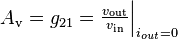 |  |
| Input resistance |  | rπ2 |
| Output resistance |  |  |
MOSFET Cascode: low-frequency small-signal parameters[4]
Similarly the small-signal parameters can be derived for the MOSFET version, also replacing the MOSFET by its hybrid-pi model equivalent. This derivation can be simplified by noting that the MOSFET gate current is zero, so the small-signal model for the BJT becomes that of the MOSFET in the limit of zero base current:
-


 ,
,

where VT is the thermal voltage.
| Definition | Expression | |
|---|---|---|
| Voltage gain | | − (gm1rO1 + 1)gm2rO2 |
| Input resistance | |  |
| Output resistance | |  |
The combination of factors gmrO occurs often in the above formulas, inviting further examination. For the bipolar transistor this product is (see hybrid-pi model):
-
 .
.
In a typical discrete bipolar device the Early voltage VA ≈ 100 V and the thermal voltage near room temperature is VT ≈ 25 mV, making gmrO ≈ 4000, a rather large number. From the article on hybrid-pi model, we find for the MOSFET in the active mode:

At the 65 nanometer technology node, ID ≈ 1.2 mA/μ of width, supply voltage is VDD = 1.1 V; Vth ≈ 165 mV, and Vov = VGS-Vth ≈ 5%VDD ≈ 55 mV. Taking a typical length as twice the minimum, L = 2 Lmin = 0.130 μm and a typical value of λ ≈ 1/(4 V/μm L), we find 1/λ ≈ 2 V, and gmrO ≈ 110, still a large value.[5] [6] The point is that because gmrO is large almost regardless of the technology, the tabulated gain and the output resistance for both the MOSFET and the bipolar cascode are very large. That fact has implications in the discussion that follows.

0 comments:
Post a Comment